Capabilities
Full Service Manufacturing Capabilities
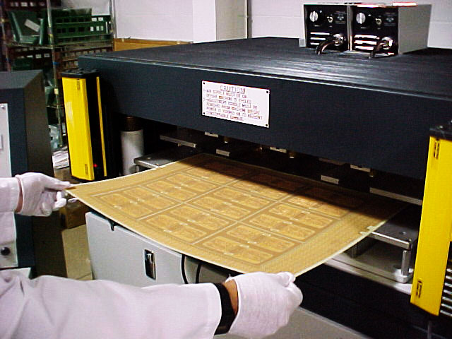
Geometric Circuits Inc. is a full service printed circuit board supplier. Below is a list of Geometric Circuits PCB manufacturing capabilities.
Geometric Circuits accepts PCB files in Gerber 274X file format and all PCB files should be sent in a zip-format and along with drawings to sales@geometriccircuits.com.
Materials Available
- FR4 (High TG)
- Teflon
- Rogers
- Aluminum Based
- Taconic
Production Tolerance |
Standard |
Advanced |
|---|---|---|
| Copper Thickness | Min 1/2 oz, Max 6 oz | Min 1/3 oz, Max 10 oz |
| Minimum Outer Line Width | .004" | .003" |
| Minimum Inner Line Width | .004" | .003" |
| Minimum Outer Space, Trace/Trace | .004" | .0035" |
| Minimum Inner Space, Trace/Trace | .004" | .0035" |
| Minimum Space, PCB Edge to Conductor | .006" | .004" |
| Layer-to-Layer Registration | +/- .003" | +/- .002" |
| Maximum Finished PCB Thickness | .200" | .250" |
| Minimum Board Thickness Tolerance | +/- 10% | +/- 6% |
| Dimensions-Fab O.D. | .005" | .004" |
| Fabrication Radius | +/- 5 deg | +/- 5 deg |
| Warp Age (inch per inch)(flatness of finished board) | 0.75% | 0.50% |
Pad to Hole Size |
Standard |
Advanced |
|---|---|---|
| Minimum Component Pitch | .010" | .008" |
| Minimum Dielectric Thickness | .006" | .004" |
| Maximum Number of Layers | 16 | 28 |
| Impedance Control | +/- 10% | +/- 5% |
Pad to Hole Size |
Standard |
Advanced |
|---|---|---|
| Tolerance - Plated Hole Size | +/- .003" | +/- .002" |
| Normal Finished Hole Size | .010" | .008" |
| Minimum Outer Non-Plated Hole to Trace Spacing | .007" | .004" |
| Minimum Inner Non-Plated | .007" | .004" |
Drilling |
Standard |
Advanced |
|---|---|---|
| Minimum Mechanical Drill Size | .008" | .008" |
| Minimum Laser Drill Size | .004" | .004" |
| Maximum Aspect Ratio | 12:01 | 16:01 |
Via Fill |
Standard |
Advanced |
|---|---|---|
| Inner Layers | Non-Conductive | Conductive |
| Outer Layers | Non-Conductive | Conductive |
Surface Finishes Available
- Lead HASL
- Lead Free HASL
- Entek Organic Coating (OSP)
- Immersion Ni/Au Minimum Thickness (ENIG)
- Immersion Silver
- Immersion Tin
- Peelable Mask
- Carbon Ink
- Gold (Ni/Au) Fingers
Other Attributes
- Blind and Buried Via's
- Laser Drilled Micro Via's
- Entek Organic Coating (OSP)
- Via Fill
On Time Delivery
Outstanding Quality
Competitive Prices